Reviewing Intel's Split: Part I
Design CAD Tool Commodification, with Wardley Maps
Intel’s changing its direction in terms of strategic competencies. The decision was to split out the design and manufacturing capabilities as external services, while at the same time continuing down their traditional strategic path of full integration of the two.
The ever excellent Stratechery offers a breakdown, including references to a fantastic paper from Intel1.
The roots of Intel’s change can be traced back to the 1980s and the revolution described in that paper. Computer Aided Design (CAD) was about to revolutionize chip design, with Intel and UC Berkley leading the charge.
At the time Moore’s law had been in full swing for a couple of decades, and the performance jumps that came from ever increasing transistor-per-IC counts was an expectation the semiconductor industry had signed up for. Intel had long realized that they were not able to continue to meet this expectation without a leap in design productivity, and had already been developing software tools to assist design.
Intel’s chip design situation at the time of the 80386 can be simplified and illustrated as a Wardley Map:
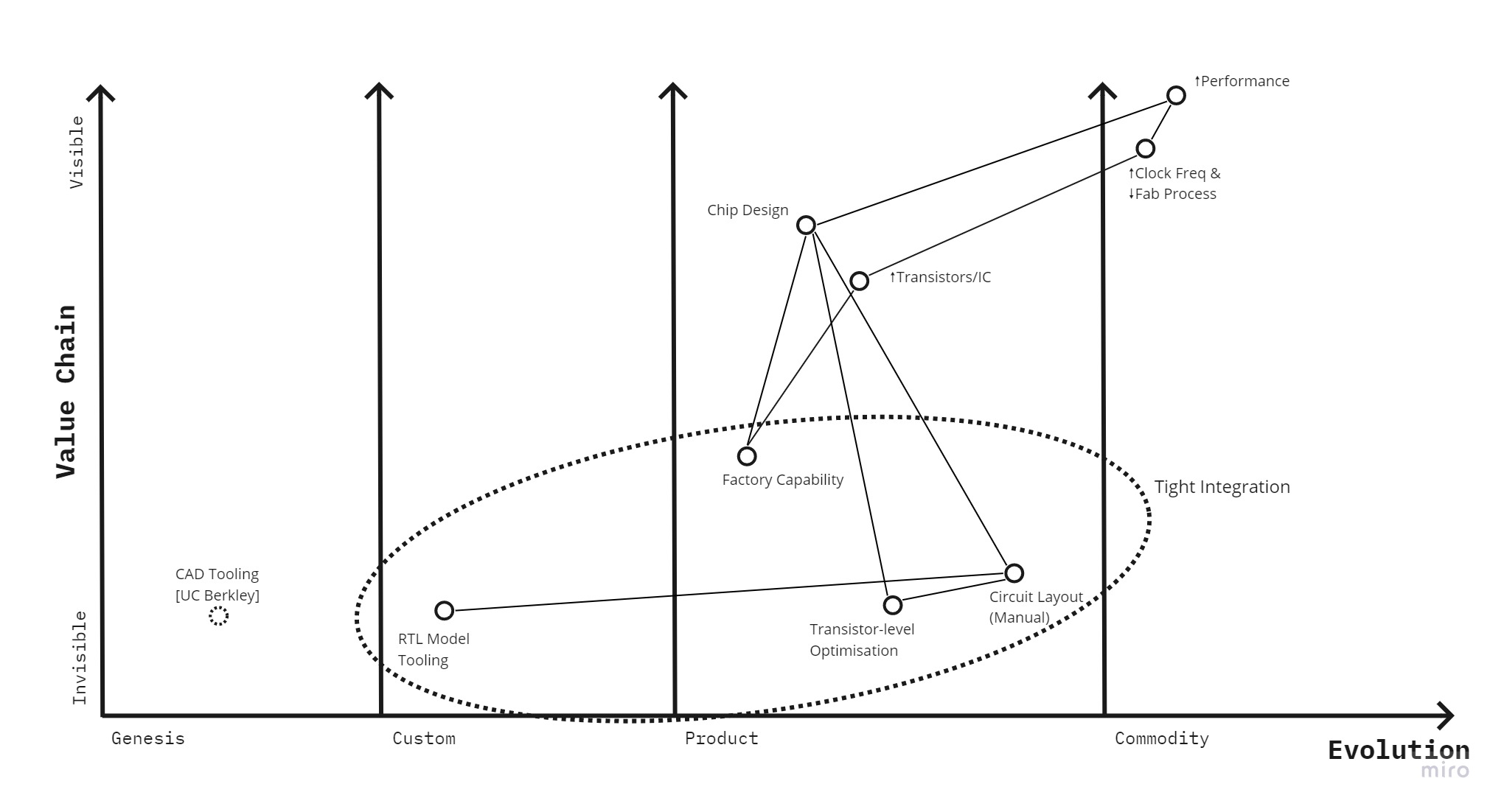 Though they had some tooling in place for many years designs were still optimized at the individual transistor level and schematics were still drawn by hand. At the same time CAD for chip design was a focus of research and innovation at UC Berkley.
For the 80486 Intel (based on work with UC Berkley and others) developed a software system to produce chip designs all the way to circuit layouts. Called RLS, it removed the need for transistor-level optimization and manual circuit diagrams, and gave them a large leap in chip design productivity. This enabled them to continue delivering on the promise of ever increasing performance of CPUs2.
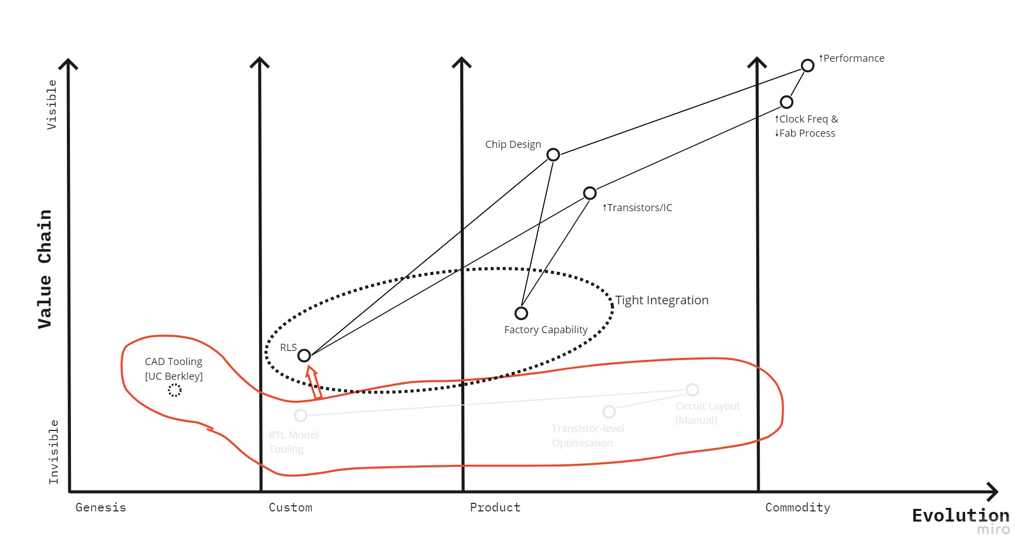
In the period of a few years, Intel set themselves up for a couple of decades of ever-improving chip designs off the back of RLS. For each engineer it was an instant game changer:
“With a combination of basic training and a set of automation tools to aid symbolic layout, productivity tripled in a matter of weeks.” This might be recognized as a standout example in the history of technology evolution, an incredible achievement at Intel that we are all the beneficiaries of.
But over those decades of Intel’s advancement the industry landscape was not staying stationary. The 80486 map above clearly shows where the commodification of CAD tools (such as RLS) could lead to a modular split of what had been an integrated business, into the design and fab arms. CAD tooling for chip design migrated from its genesis to be standardized by the industry. In a similar manner, a chip foundry became a product (as per TSMC) as did chip design (as per ARM).
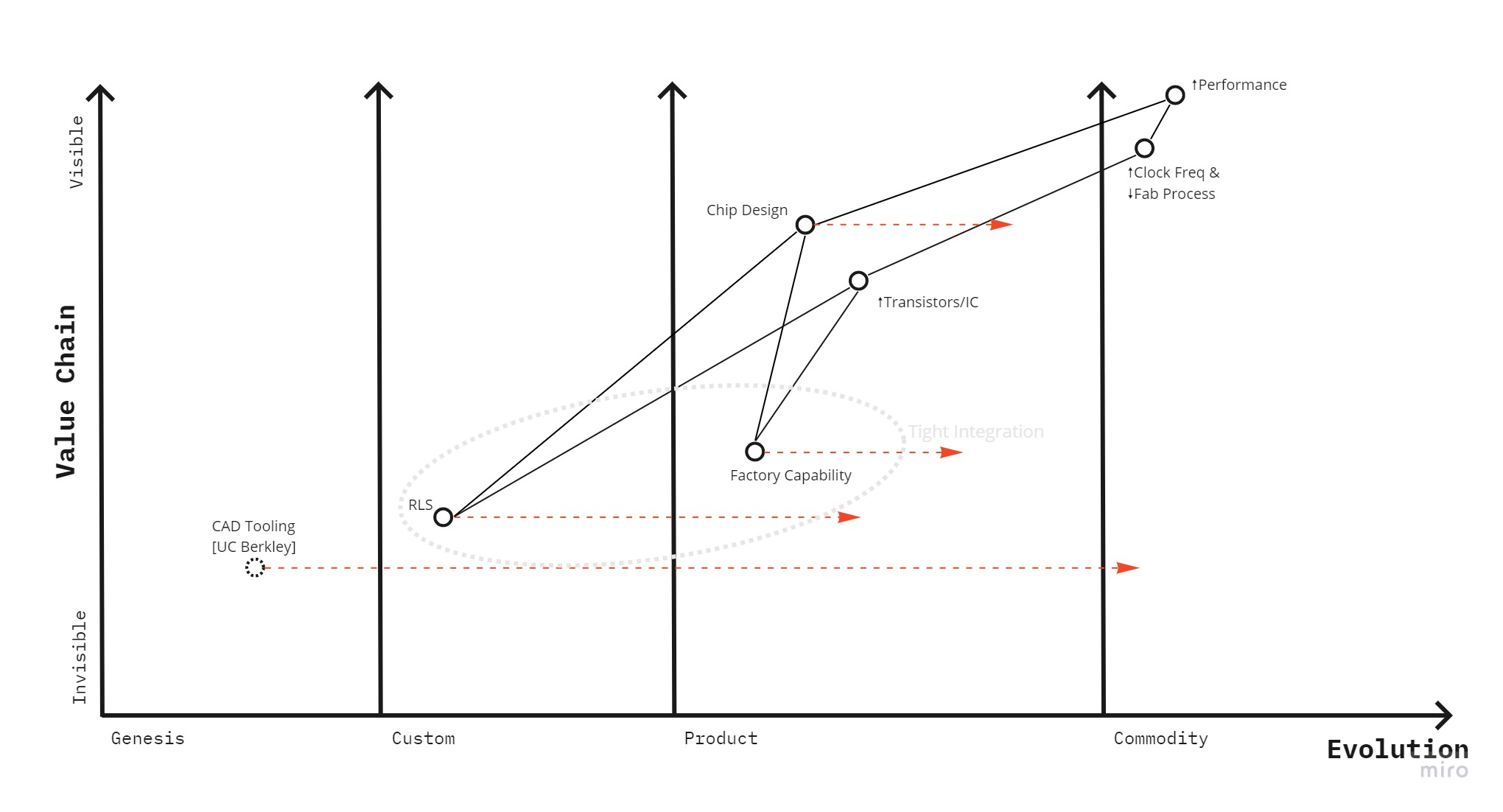
Now days fab-less design companies and foundry-only companies dominate the semiconductor industry. Looking back, we can see how a Wardley map of the landscape and prevailing climate patterns may have predicted Intel’s eventual split.
In Part II we will describe this in terms of Clayton Christensen’s theories of disruption and conservation of attractive profits.
-
You don’t need a semiconductor background to get a lot from reading that paper. It lays out an extraordinary period of challenge and lasting change, in an approachable format that folds together technical leadership insights and warm anecdotes. Any indulgences are forgiven; it is easy to join the dots from the 1980s overhaul of chip design to the worldwide revelations of the Internet, mobile and more. ↩︎
-
Read the paper for some of the glimpses into the difficulty encountered along the way. In Wardley-speak they had to break through significant inertia. ↩︎